When making custom electronics, producing a quality enclosure for the boards can make any project look more professional. There are a large range of enclosures which use end panels, such as the Hammond 1593 series, which can be replaced by custom panels fabricated using standard PCB production techniques. The result is a good looking enclosure with a minimum of manufacturing time and at a very reasonable cost. Despite the ease of producing these I have seen very few designs using this technique, so have produced this guide to provide some insight into the process behind making them for one of my recent projects, A Morse code side-tone generator for amateur radio, details of the project can be found on the Southampton University Wireless Society Website.
With this style of enclosure there are a couple of other options which may also be applicable to your design. The other options I considered were laser cutting a new panel or CNC milling/drilling the ones included with the case, but both of these require additional manufacturing steps which I wanted to avoid on this project. Designing panels for these techniques follows most of the same steps as below but differs at the production steps.
Completed project with PCB panels
Workflow for creating the front panel.
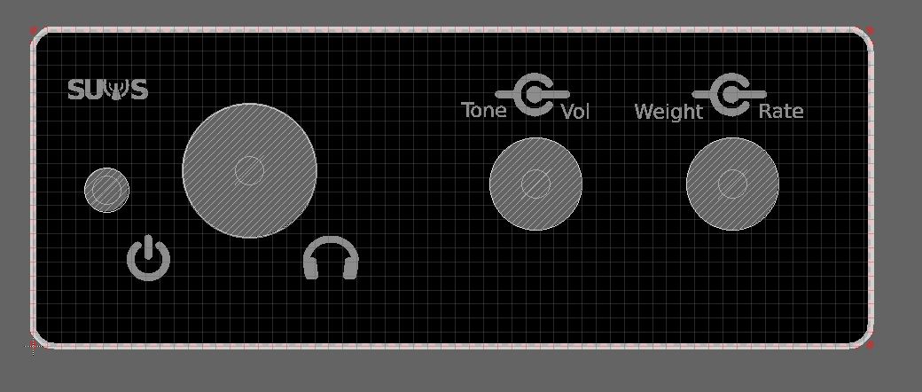
The first step in creating the panel is to work out what connectors, buttons, and other components need to be available through the front panel. In the case of this project there were a few connectors, a pair of potentiometers and a status LED. I modeled these in Inventor (a 3D modeling package) along with the PCB outline and imported the models for the enclosure (most enclosure manufacturers have CAD models available for download). An assembly was created with all the required parts. The placement of the mechanical components can then be determined, make sure to check the depth of the components at this point as some will not want to align with the edge of the board such as the 1/4in jacks that wanted to be set slightly back. The existing panels in the enclosure CAD model can then be replaced with a new part created with the required cutouts for the connectors and interfaces.
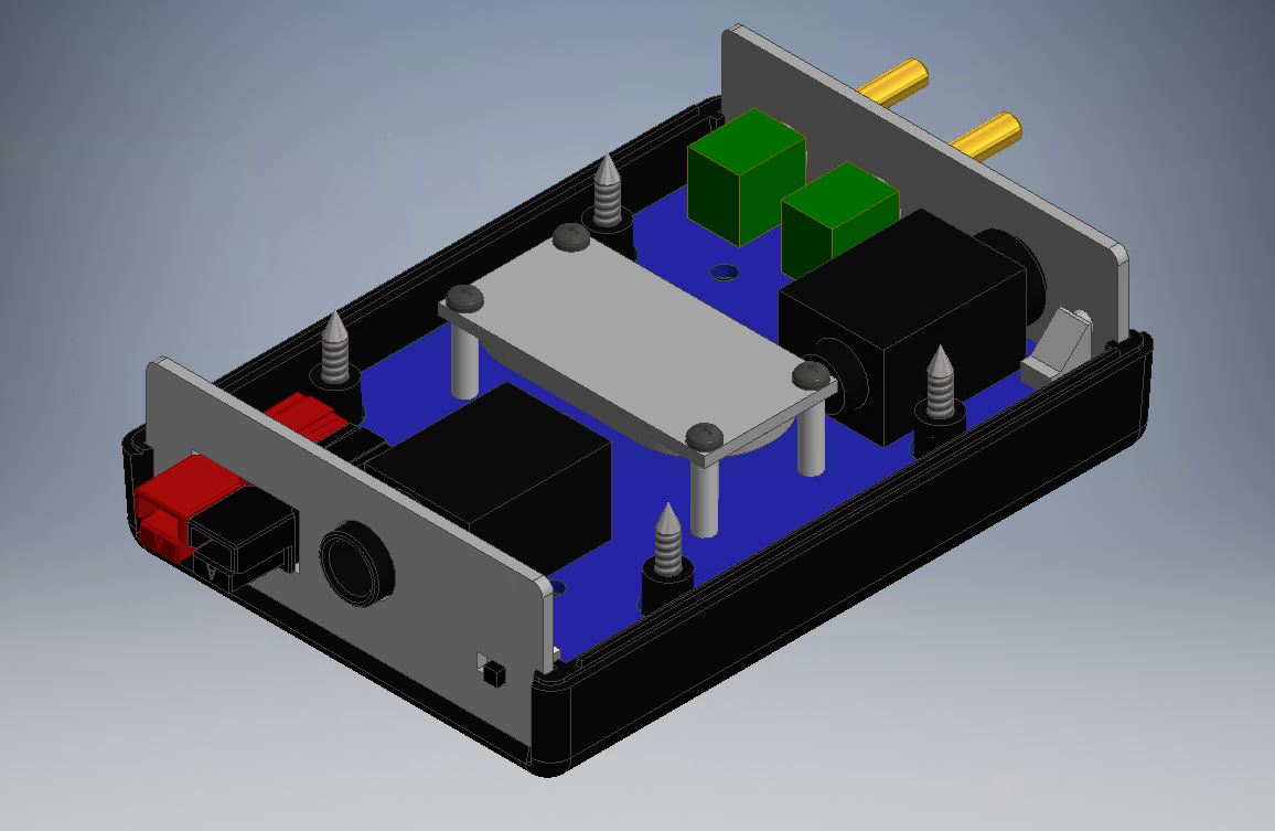
Inventor model of sounder with mechanical components
Once the mechanical components locations have been decided, these can be placed onto the PCB at the positions determined by the 3D design. The rest of the PCB can then be laid out as usual.
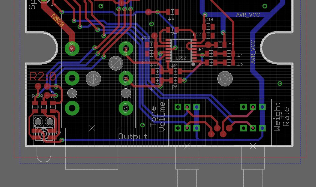
PCB with aligned front panel components
For the panel design I exported the face of the panel to a DXF and imported the outline into Inkscape. In Inkscape I added the artwork for the front panel which would end up on the silk and soldermask layers of the PCB. The artwork was exported from Inkscape and imported as a bitmap into Eagle along with the DXF of the outline. The layers are adjusted in Eagle so the artwork appears on the correct layers, the labels are on the silkscreen layer which will come out as white while the SUWS logo is in the soldermask layer meaning it will come out in silver.
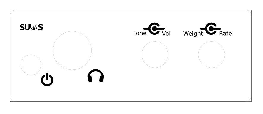
 Panel designs in Inkscape and when imported into Eagle
The panels can then be attached to the rest of the PCB with breakout tabs and ordered at the same time. Assembly is as simple as cutting them off the boards and putting them into the case. On this project I was also able to go further and used some extra PCB space to build a functioning capacitive morse key with all the circuitry on the front panel, this was done with much the same process as above but with the electronics placed on the back of the panel design.
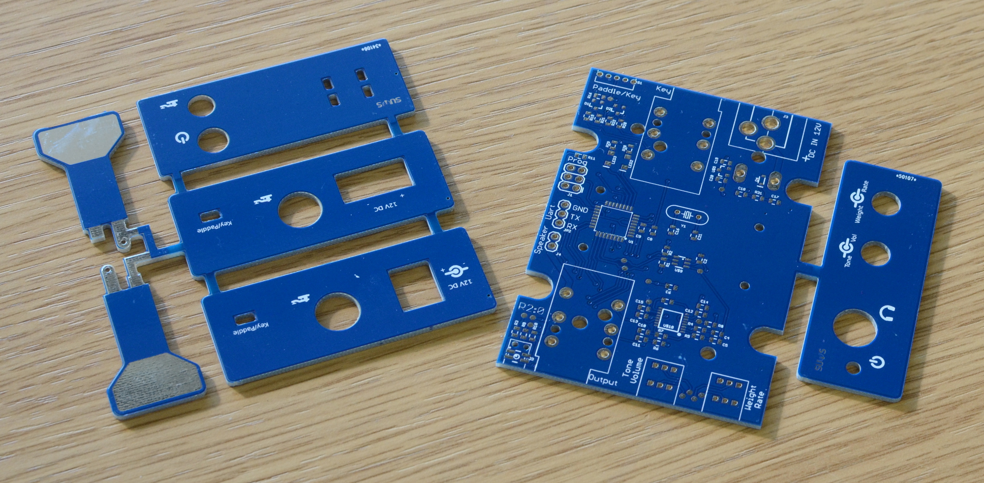
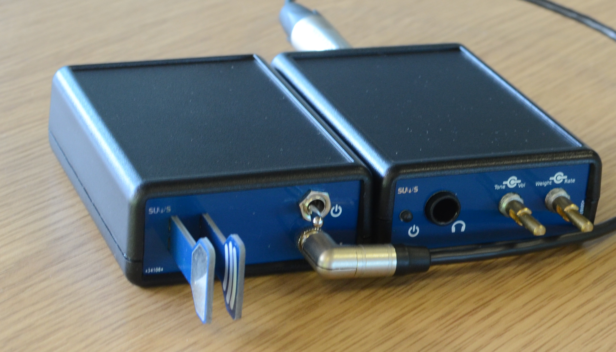
Completed PCB panels
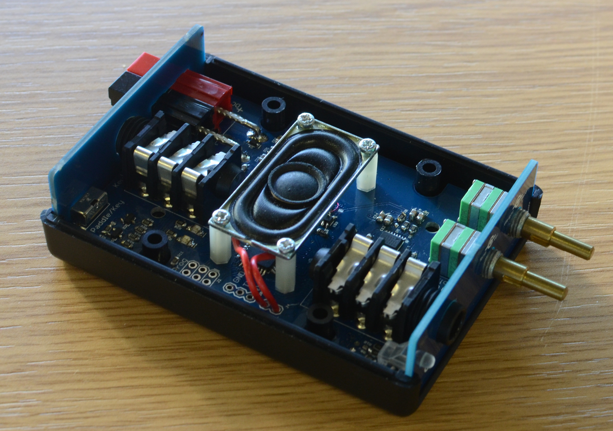
Completed board with panels installed
Pingback: Morse sounder project complete | SUWS - Southampton University Wireless Society
The word Panel is spelled incorrectly (with two ns) in the title of this post. This has propagated quite widely on this and other pages.
Good article by the way.
Another great write-up! We love audio projects and use the same CAD tools. We should have a chat sometime about some collaboration ideas!
Happy to chat about a collaboration. Projects I do for this blog do often tend to take a while to complete however, due to a limited amount of spare time to work on them so might not be particularly quick depending on what you had in mind. Feel free to drop me an email, tyler@ this domain will get to me.